A Comprehensive Tutorial on Bipolar Junction Transistors for Electronics Engineering
Introduction
Bipolar Junction Transistors (BJTs) are fundamental components in electronics engineering. They are used in a wide range of applications, including amplifiers, oscillators, and switches. This tutorial aims to provide a comprehensive understanding of how BJTs work, along with the necessary mathematical expressions to analyze their behavior. We’ll be covering the basics of BJT operation, the different configurations, and the key parameters that govern their performance.
Basics of Bipolar Junction Transistors
A BJT is a three-layer semiconductor device consisting of two pn-junctions, which are formed by sandwiching either a p-type or an n-type material between two oppositely doped layers. There are two types of BJTs: NPN and PNP.
1.1 NPN Transistor
Symbol:

Layers: Emitter (n-type), Base (p-type), Collector (n-type)
1.2 PNP Transistor
Symbol:
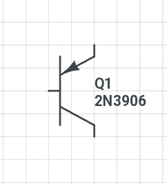
Layers: Emitter (p-type), Base (n-type), Collector (p-type)
BJT Configurations
There are three primary BJT configurations: Common Base (CB), Common Emitter (CE), and Common Collector (CC).
2.1 Common Base (CB)
Input: Emitter-Base
Output: Collector-Base
2.2 Common Emitter (CE)
Input: Base-Emitter
Output: Collector-Emitter
2.3 Common Collector (CC)
Input: Base-Collector
Output: Emitter-Collector
BJT Operation
In this section, we will focus on the NPN transistor in the common emitter configuration, as it is the most widely used. The same principles apply to PNP transistors with appropriate polarity changes.
3.1 Active Region
When the base-emitter junction is forward-biased and the base-collector junction is reverse-biased, the transistor operates in the active region. In this region, a small base current (IB) controls a much larger collector current (IC). The relationship between these currents is described by the current gain (β), also known as the DC current gain or the hFE parameter.
IC = β × IB
3.2 Saturation Region
When both the base-emitter and base-collector junctions are forward-biased, the transistor operates in the saturation region. In this region, the transistor acts as a closed switch, allowing maximum current to flow from the collector to the emitter.
3.3 Cut-off Region
When the base-emitter junction is reverse-biased or no base current is flowing, the transistor is in the cut-off region. In this region, the transistor acts as an open switch, with no collector current flowing.
Key BJT Parameters
4.1 DC Current Gain (β or hFE)
As mentioned earlier, the DC current gain is the ratio of the collector current (IC) to the base current (IB).
β = IC / IB
4.2 Input Impedance (Zin)
Input impedance is the ratio of the input voltage (Vin) to the input current (Iin). For the common emitter configuration, the input impedance can be calculated as:
Zin = Vin / Iin = (VBE + VRE) / IB
4.3 Output Impedance (Zout)
Output impedance is the ratio of the output voltage (Vout) to the output current (Iout). For the common emitter configuration, the output impedance can be calculated as:
Zout = Vout / Iout = VCE / IC
4.4 Voltage Gain (Av)
Voltage gain is the ratio of the output voltage (Vout) to the input voltage (Vin). For the common emitter configuration, the voltage gain can be calculated as:
Av = Vout / Vin = (RC / (RC + RE)) × (β × RE)
4.5 Power Gain (Ap)
Power gain is the product of the current gain (β) and the voltage gain (Av). For the common emitter configuration, the power gain can be calculated as:
Ap = β × Av
Conclusion
This comprehensive tutorial on bipolar junction transistors for electronics engineering has covered the basics of BJT operation, different configurations, and key parameters that govern their performance. With this knowledge, you can now analyze and design circuits involving BJTs for various applications, such as amplifiers, oscillators, and switches. Remember that the same principles apply to both NPN and PNP transistors, with appropriate polarity changes. Happy designing!
